
SDC #
What is SDC? #
The Synopsys Design Constraints (SDC) format specifies design intent, including timing, power and area constraints for a design. This format is used by different EDA tools to synthesize and analyse a design. SDC is based on tool command language (TCL).
Why SDC is essential? #
We have verilog, VHDL etc. to define the design’s functionality, which will be verified using complex math in test benches. What about the timing, will it meet the timing ?
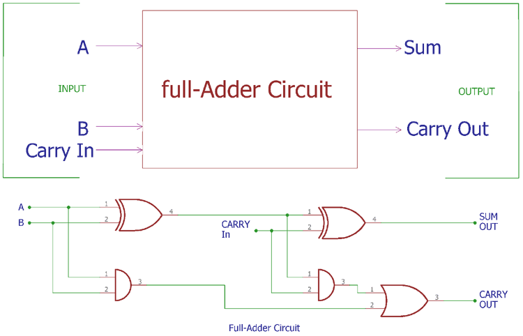
Taking an example of adder,
In HDL languages, the description only describes the design’s functionality.
An adder is more than adding two numbers. In terms of functionality, it’s just enough. However, it must happen at a certain point. Our design has a specific target frequency based on the specification. It is necessary to reach a certain frequency. Therefore we need a language to define timing requirements called SDC timing constraints.
We ensured that our design was functionally correct, and these functions should work at the required speed.
When we have done the simulation, the design functionally is fine. Simulation didn’t consider timing. Earlier in the synthesis process, some estimated values are used to calculate but later once place and route are considered, timing is more accurate. Additionally, our design needs to include physical timing information. Which means SDC timing is also part of the source code like RTL.
· RTL is the source code for functional requirements, while SDC is the source code for timing requirements.
When we opt for big SOC designs having multi-million gates we have complex SDC constraints.
What about Gate simulation, and why can’t we use it instead?
Gate level simulation can run functional simulations including timing. But we can check every path and node for timing in small designs, but it can’t be done for more complex ones. And also gate level simulation is so slow.
The SDC is very useful for defining the timing requirements for the static timing analysis, since it is a static method. Today, every STA tool is based on SDC.
SDC constraints role in synthesis optimization
Take the example of an adder.
In order to implement an adder, which type of adder should be inferred is the biggest decision for logic synthesizers.
Ripple carry adder is adder in which the carry ripples to calculate each bit carry in. The circuit is so small, but it consumes a lot of time.
Whereas carry lookheader calculates carry and the circuit is so big but so fast.If we provide the SDC constraints it will guide the synthesizer to choose which needs to be implemented
SDC file contains the following information:
SDC version (optional) #
This statement specifies the SDC file version. It could be 2.1, 2.0, 1.9 or more older.
Example:
set sdc_version 2.1
SDC units (optional) #
Units of various quantities like time, resistance, capacitance, voltage, current, and power can be specified using the set_unit command.
Multiple units can be set using a single set_unit command.
Example:
set_units -time ns -resistance Kohm -capacitance pF -voltage V -current mA
- Design constraints
- Design objects
- Comments (optional)
Design constraints include operating conditions, wire load models, system interfaces, design rule constraints, timing constraints, timing exceptions, area constraints, multi-voltage & power optimization constraints and logic assignments.
Design constraints will have all object access commands. Objects can be design, clock, port, pin, cell, net, library, etc.
We will understand the design constraints with reference to the following figure. We will not look at SDC commands syntax. The aim is to understand how an SDC file is written for a design.

There are two blocks in the design named block A and block B. The design uses two PLLs for two different clocks. Design constraints will be defined at the I/O pins.
I/O Pins 2, 6, 10 – Clocks are the most significant part of a design. As there are two PLLs in the above design, it is clear that there are two different clocks in the design. Timing constraints must specify these clocks. At pin IO2 of block A and pin IO6 of block B, the clocks enter the blocks. The pins are therefore defined using the create_clock command. This command specifies the period, duty cycle, rise and fall edges of a clock. You can also name the clock. Clock CK1 also goes to the clock pins of the flops in block2. So, we have to define clock CK1 at IO10 of block 2 as well.
E.g. create_clock -period 10 -waveform {0 6} -name my_clk1 [get_ports IO2]
I/O Pin 1 – The input port is set with the command set_driving_cell. Doing this causes the port to have a cell delay that is a load-dependent value of the external cell driving that port. In the design shown in the figure, the buffer is an external cell that drives block A’s input port. Doing this helps us have accurate external delay for timing calculations.
E.g. set_driving_cell -lib_cell BUF [get_ports IO1]
Clock generators 3, 7 – There can be several clock generator circuits in the given design. The frequency of these generated clocks is different from the master clock. Clock generators can be used for multiplying, dividing or inverting the master clock to derive the generated clock. As frequency changes, we define them as new generated clocks at the output of the clock generator circuit. The create_generated_clock command is used for this
Purpose. While defining the generated clock, we must specify the master clock.
E.g. create_generated_clock -divide_by 2 -source [get_ports IO2] -name clk_div [get_registers FF2]
I/O Pin 4 – To do constraint checking at the output port, the set_output_delay command is used. This command calculates the delay between the output port and the next sequential cell (which captures data from this output port). But when we think about block level design, we will not know where the output port is connected. Still we should calculate the output delay. To make this possible, a virtual clock is defined. This virtual clock is the same as a normal clock but has no real existence.
E.g. set_output_delay 1.7 -clock my_clk1 [all_outputs]
I/O Pin 5 – Similar to output delay, input delay is calculated by the set_input_delay command to calculate the timing requirements at the input port. It will calculate the timing of the external path to the input port.
I/O Pin 11 – set_load command describes an external load capacitance connected to the top level port. This command considers pin and wire capacitance. This command helps us time the design accurately.
E.g. set_load 20 [get_ports IO11]
As there are two different clocks (i.e. asynchronous clocks) in the design, any path that starts at CK1 and connects to CK2 should not be considered for timing analysis. Set_clock_group specifies whether clock groups are synchronous, asynchronous or exclusive, which is the best way to achieve this.
In this example, CK1 and CK2 are set as asynchronous clocks. In block 2, output of the mux goes to FF5. Inputs to the mux are CK2 and a generated clock with CK2 as a master clock. But at a particular time, only one clock will go to a mux output. Hence, these two clocks are set mutually exclusive.
Timing Exceptions: #
1. False path:
Some paths in the design need not be considered for timing analysis. There can be multiple reasons to set a path as a falsepath. One of the reasons is shown in the above design. CK1 and CK2 are asynchronous clocks, so we set any path from CK1 to CK2 as a falsepath. The set_false_path command is used for this purpose. Path from FF4 to FF5 is a false path because both flops are driven by different clocks.
E.g. set_false_path -from [get_clocks my_clk1] -to [get_clocks my_clk2]
2. Max & Min path:
I/O Pins 8, 9 – The path groups are of four types: input-to-reg, reg-to-output, reg-to-reg and input-to-output. The path from input pin IO8 to output pin IO9 of block A is input-to-output. In such cases, we have to constrain these paths to maximum or minimum delay. The set_max_delay and set_min_delay commands define these delays.
E.g. set_max_delay 0.15 -from IO8 -to IO9
3. Multi-cycle path:
Data takes one clock cycle to propagate from launch flop to capture flop. But it can also take more than one clock cycle. We should set such paths to multi-cycle paths using the set_multicycle_path command. Multi-cycle path is always a multiple of the clock cycle.
Setting clock transition #
Set_clock_transition –rise 0.05 [get_clocks test_clock]
Set_clock_transition –fall 0.08 [get_clocks test_clock]

Clock Uncertainty #
set_clock_uncertainty -setup 0.01 [get_clocks CLK_CONFIG]
set_clock_uncertainty -hold 0.002 [get_clocks CLK_CONFIG]

Interclock uncertainty #
set_clock_uncertainty -from SYS_CLK -to CFG_CLK -hold 0.05
set_clock_uncertainty -from SYS_CLK -to CFG_CLK -setup 0.1

Clock Latency:
set_clock_latency 1.2 -rise [get_clocks TEST_CLK]
set_clock_latency 1.8 -fall [all_clocks]
set_clock_latency 0.851 -source -min [get_clocks CFG_CLK]
set_clock_latency 1.322 -source -max [get_clocks CFG_CLK]

Generated Clock:
There are two types of generated clocks:
#1. Divide By Clock
#2. Multiply By Clock
Divide By Clock
create_generated_clock -name TEST_CLK_DIV2 -source TEST_PLL/CLKOUT -divide_by 2 [get_pins UFF0/Q]

Multiply By Clock
create_generated_clock -name PCLKx2 -source [get_ports PCLK] -multiply_by 2 [get_pins UCLKMULTREG/Q]

set_case_analysis #
Specifies constant value on a pin of a cell, or on an input port.
set_case_analysis 0 [get_ports {testmode[3]}]


