
Sequential Logic #
- Combinational logic refers to circuits whose output is strictly depended on the present value of the inputs, circuits have no memory. In many applications, information regarding input values at a certain instant of time is required at some future time.
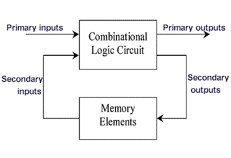
- Circuits whose outputs depend not only on the present input value but also the past input value are known as sequential logic circuits. The mathematical model of a sequential circuit is usually referred to as a sequential machine.
A general block diagram of a sequential circuit is shown below in Figure.
- Sequential circuits are divided into two main types: synchronous and asynchronous. Their classification depends on the timing of their signals.
- Synchronous sequential circuits change their states and output values at discrete instants of time, which are specified by the rising and falling edge of a free-running clock signal.
- In asynchronous sequential circuits, the transition from one state to another is initiated by the change in the primary inputs; there is no external synchronisation.

Latch #
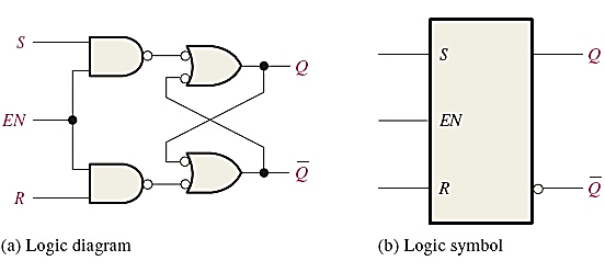
- A latch is a temporary storage device that has two stable states (bistable). It is a basic form of memory. The S-R (Set-Reset) latch is the most basic type. It can be constructed from NOR gates or NAND gates.
- With NOR gates, the latch responds to active-HIGH inputs; with NAND gates, it responds to active-LOW inputs. Logic diagrams and symbols are shown below:


Set state: Q = 1, Q’ = 0 Clear state: Q = 0, Q’ = 1
| NOR Gate SR Latch | ||||
| S | R | Q | Q’ | |
| 1 | 0 | 1 | 0 | |
| 0 | 0 | 1 | 0 | (after S=1, R=0) |
| 0 | 1 | 0 | 1 | |
| 0 | 0 | 0 | 1 | (after S=0, R=1) |
| 1 | 1 | 0 | 0 | Undefined |
| NAND Gate SR Latch | ||||
| S | R | Q | Q’ | |
| 1 | 0 | 0 | 1 | |
| 1 | 1 | 0 | 1 | (after S=1, R=0) |
| 0 | 1 | 1 | 0 | |
| 1 | 1 | 1 | 0 | (after S=0, R=1) |
| 0 | 0 | 1 | 1 | Undefined |
- The active-HIGH S-R latch is in a stable (latched/no change) condition when both inputs are LOW. The active-LOW S-R latch is in a stable (latched/no change) condition when both inputs are HIGH.
- Assume an active-HIGH latch is initially RESET (Q = 0) and the inputs are at their inactive level (0). To SET the latch (Q = 1), a momentary HIGH signal is applied to the S input while the R remains LOW. To RESET the latch (Q = 0), a momentary HIGH signal is applied to the R input while the S remains LOW. Never apply an active set and reset at the same time (invalid).
- The gated latch has an additional input, called enable (EN) that must be HIGH in order for the latch to respond to the S and R inputs.
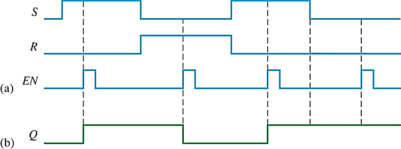
- Assume Q starts LOW, the following figure shows the Q output with relation to the input signals. Keep in mind that S and R are only active when EN is HIGH.
The state of the latch is free to change as long as CP (same as Enable E) is equal to 1.

SR Latch With Control Input #
| SR Latch With Control | |||
| CP | S | R | Q(t + 1) |
| 0 | X | X | no Change |
| 1 | 0 | 0 | no Change |
| 1 | 0 | 1 | Q=0 (Reset) |
| 1 | 1 | 0 | Q=1 (Set) |
| 1 | 1 | 1 | Indeterminate |
Q (t + 1) = S + R’Q
The D latch is a variation of the S-R latch but combines the S and R inputs into a single D input as shown:

A simple rule for the D latch is: Q follows D when the Enable is active.

The truth table for the D latch summaries its operation. If EN is LOW, then there is no change in the output and it is latched.
| Inputs
D EN |
Outputs
Q Q’ |
Comments |
| 0 1 | 0 1 | RESET |
| 1 1 | 1 0 | SET |
| X 0 | Q0 Q’0 | No Change |
Flip Flops #
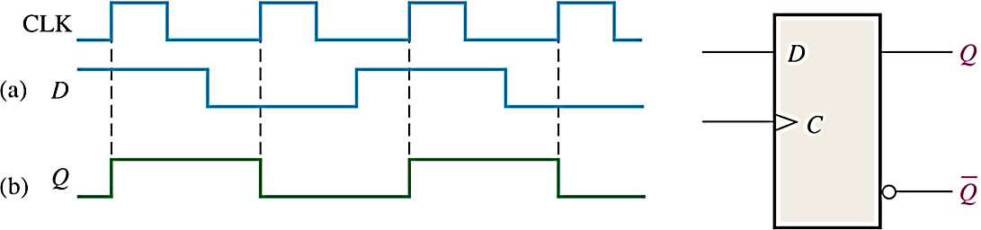
- A flip-flop differs from a latch in the manner it changes states. A flip-flop is a clocked device, in which only the clock edge determines when a new bit is entered.
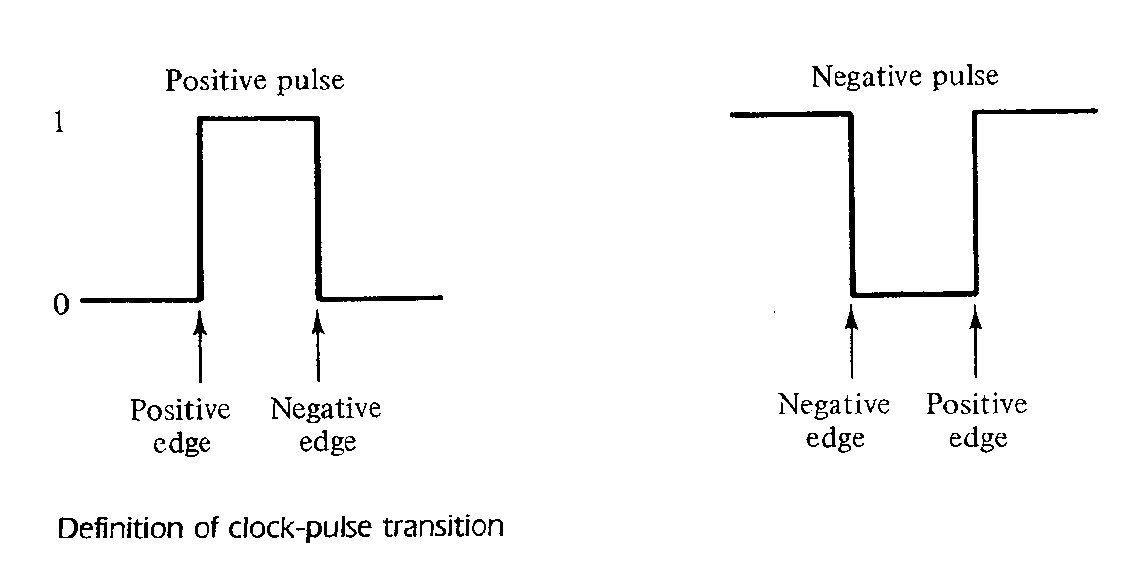
- The active edge can be positive or negative.
- The truth table for a positive-edge triggered D flip-flop shows an up arrow to remind you that it is sensitive to its D input only on the rising edge of the clock; otherwise it is latched (no change). The truth table for a negative-edge triggered D flip-flop is identical except for the direction of the arrow.
| Inputs
D CLK |
Outputs
Q Q’ |
Comments |
| 1 ↑ | 1 0 | SET |
| 0 ↑ | 0 0 | RESET |
Edge-Triggered D Flip-Flop #
- Edge triggered flip-flops respond only to a clock pulse edge and not to the level of the of the clock pulse.
- Edge-triggered flip-flops can be either positive or negative edge sensitive.
- One type of edge-triggered flip-flop is the master-slave flip-flop. It is constructed from two separate flip-flops and an inverter.
- The master latch is triggered on the leading edge of the clock pulse and the slave on the trailing edge.
- Only one latch is enabled at a time.
- The master latch is enabled when the clock input is high and the slave is enabled when it is low. This behavior could be reversed with the addition of an inverter on the clock input.
- In a master-slave flip-flop, it is possible to switch the output of the flip-flop and its input information with the same clock pulse.
- The master-slave combination can be constructed for any type of flip-flop by adding a clocked SR latch with an inverted clock to form the slave.

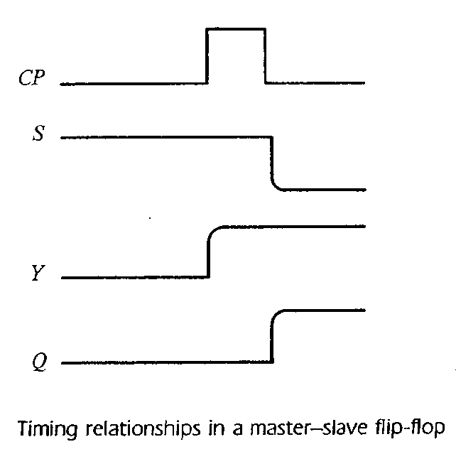
Timing relationships in a master – slave flip-flop
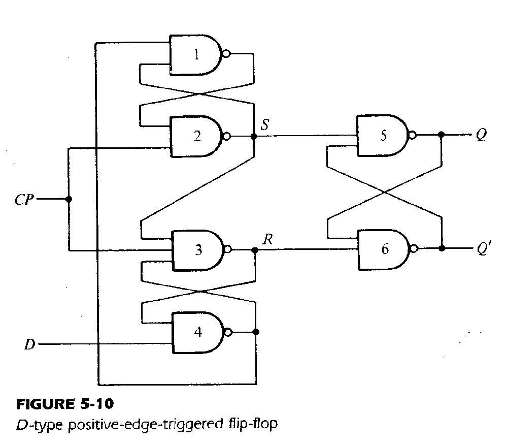
- A more efficient construction of an edge-triggered D flip-flop uses three SR latches.
- In this design, two latches respond to the external data and clock inputs. The third latch provides the outputs for the flip-flop.
- The S and R inputs of the output latch are maintained at a logic 1 level when CLK = 0. This causes the output to remain in its present state.
- If D = 0 when CLK becomes 1, R changes to 0, resetting the output latch (Q = 0). If there is a change in D while CLK = 1, R remains 0, locking out further change.
- When CLK returns to 0, R changes to 1, placing the output latch in the quiescent state without changing its output.
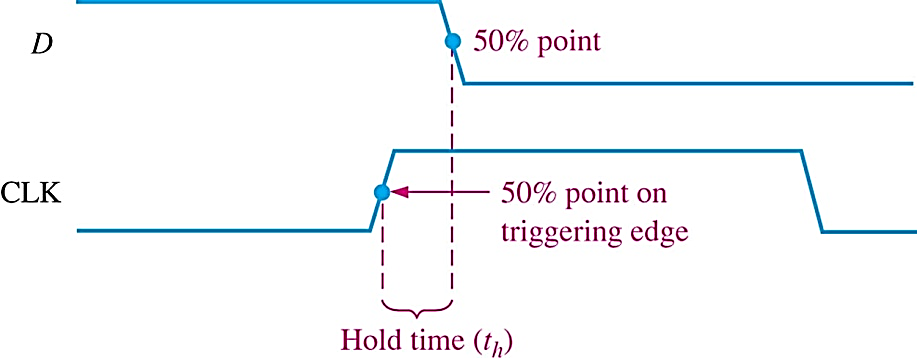
- Setup time is the time period the input must be held stable before the clock edge occurs.
- Hold time is the time period the input must be held stable after the clock edge occurs.
JK flipflop #
The J-K flip-flop is more versatile than the D flip flop. In addition to the clock input, it has two inputs, labeled J and K. When both J and K = 1, the output changes states (toggles) on the active clock edge (in this case, the falling edge).
| Inputs
J K CLK |
Outputs
Q Q’ |
Comments |
| 0 0 ↓ | Q0 Q0’ | No Change |
| 0 1 ↓ | 0 1 | RESET |
| 1 0 ↓ | 1 0 | SET |
| 1 1 ↓ | Q0’ Q0 | TOGGLE |

A JK flip-flop is a refinement of the SR latch in that the indeterminate state of the SR type is defined in the JK type.
Inputs J and K behave like inputs S and R to set and clear the flip-flop, respectively.
When both inputs J and K are equal to 1, the flip-flop switches to its complement state, i.e., if Q = 1 it switches to Q = 0, and vice versa.
The plain JK flip-flop has a serious drawback.
T Flip-Flops #
The T flip-flop is a single input version of the JK flip-flop.
The T flip-flop is obtained from the JK flip-flop by connecting the J and K inputs together.
The ‘T’ stands for “toggle”, because when the T input is equal to 1, the output will switch to its complement state.
T flip-flops have the same drawback alluded to earlier with the JK flip-flops.
Synchronous inputs (for example the D or J-K inputs) are transferred in the triggering edge of the clock. Most flip-flops have other inputs that are asynchronous, meaning they affect the output independent of the clock. Two such inputs are normally labeled preset (PRE) and clear (CLR). These inputs are usually active LOW. A J-K flip flop connected in a toggle mode with active LOW preset and CLR is shown below:


Flip Flop Characteristics #
Propagation delay time is specified for the rising and falling outputs. It is measured between the 50% level of the clock to the 50% level of the output transition.

Set-up time and hold time are times required before and after the clock transition that data must be present to be reliably clocked into the flip-flop.
Setup time is the minimum time for the data to be present before the clock.

Hold time is the minimum time for the data to remain after the clock.
- Other specifications include maximum clock frequency, minimum pulse widths for various inputs, and power dissipation. The power dissipation is the product of the supply voltage and the average current required.
- A useful comparison between logic families is the speed-power product which uses two of the specifications discussed: the average propagation delay and the average power dissipation.
Counters #
Asynchronous Counters #
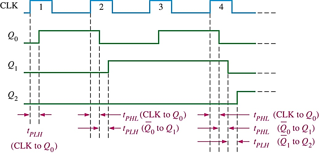
- In an asynchronous counter, the clock is applied only to the first stage. Subsequent stages derive the clock from the previous stage. The three-bit asynchronous counter shown is typical. It uses three J-K flip-flops in the toggle mode.
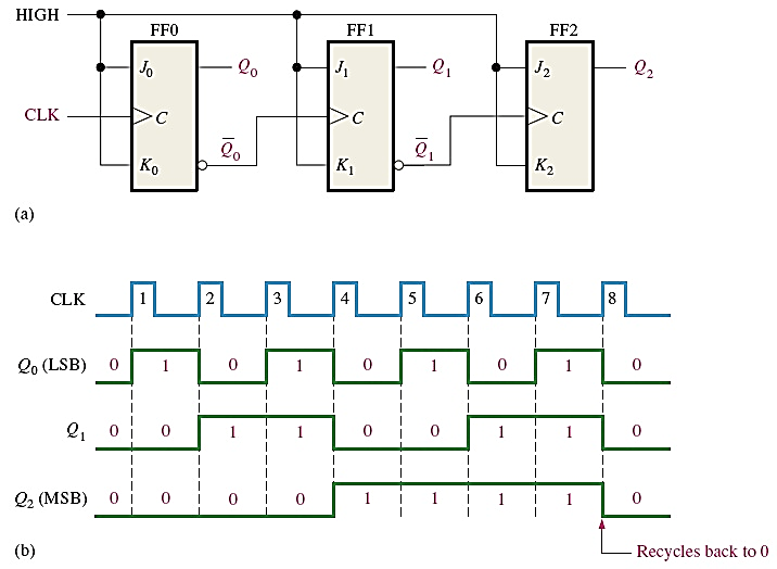
- Notice that the Q0 output is triggered on the leading edge of the clock signal. The following stage is triggered from Q0. The leading edge of Q0` is equivalent to the trailing edge of Q0. The resulting sequence is that of a 3-bit binary counter.
- Asynchronous counters are sometimes called ripple counters, because the stages do not all change together. In following figure, notice how delays are cumulative as each stage in a counter is clocked later than the previous stage.
- The maximum clock frequency at which the counter can be operated is limited by the total cumulative propagation delay. For certain applications requiring high clock rates, this is a major disadvantage
Asynchronous Decade Counter #
- This counter uses partial decoding to recycle the count sequence to zero after the 1001 state. The flip-flops are trailing-edge triggered, so clocks are derived from the Q outputs. Other truncated sequences can be obtained using a similar technique.

When Q1 and Q3 are HIGH together, the counter is cleared by a “glitch” on the CLR` line.
5.3.3 Synchronous Counter #
- In synchronous counter all flip-flops are clocked together with a common clock pulse. Synchronous counters overcome the disadvantage of accumulated propagation delays, but generally they require more circuitry to control states changes. A three bit synchronous counter logic diagram and its outputs waveform are shown below:
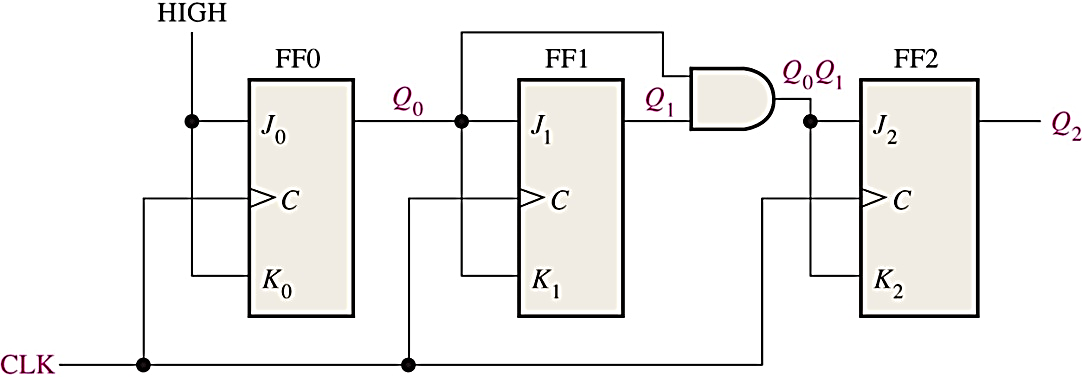

- Q0 changes on each clock cycle, Q1 changes each time Q0 is HIGH (this change occurs at clocks 2, 4, 6, and 8), Q2 changes each time both Q0 and Q1 are HIGH (this condition is detected by the AND gate and occurs at clocks 4 and 8).
Decade Synchronous Counters #
With some additional logic, a binary counter can be converted to a BCD synchronous decade counter. After reaching the count 1001, the counter recycles to 0000. An extra AND is used to detect state 1001, and causes FF3 to toggle on the next clock pulse. FF0 toggles on every clock pulse. Thus, the count starts over at 0000.

The timing waveforms of the decade synchronous counter Q0, Q1, Q2, and Q3 are shown below:

Notice that:
- Q0 : toggle on each clock
(J0 = K0 =1)
- Q1 : toggle on the next clock pulse each time Q0=1 & Q3=0
(J1 = K1 = Q0 Q3`)
- Q2 : toggle on the next clock pulse each time both Q0=1 & Q1=1
(J2 = K 2 = Q0 Q1)
- Q3 : toggle on the next clock pulse each time Q0=1 & Q1=1 & Q2 =1 (state 7) OR
when both Q0=1 & Q3=1 (state 9)
(J3 = K3 = Q0 Q1 Q2 + Q0 Q3)
Up/Down Counter #
An up/down counter is capable of progressing in either direction depending on a control input UP/DAWN`.

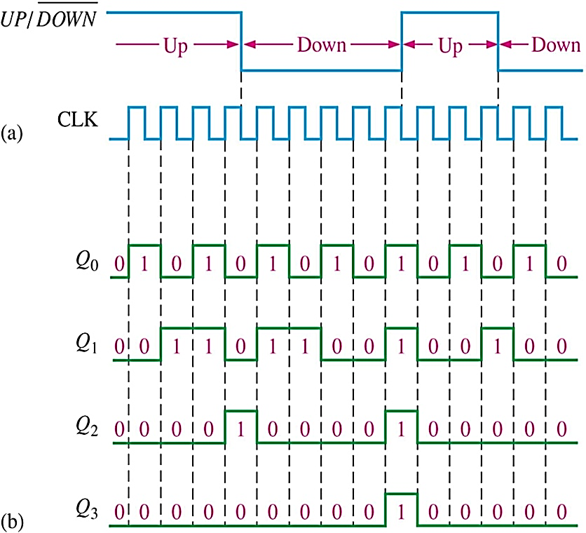
The timing waveforms of the UP/DOWN synchronous counter Q0, Q1, and Q2 are showing that:
- Q0 : toggle on each clock
J0 = K0 = 1
- Q1 :
- for the UP sequence toggles on the next clock when Q0 =1
- for the DAWN sequence toggles on the next clock when Q0 =0
J1 = K1 = (Q0 . UP) + (Q0` . DOWN)
- Q2 :
- for the UP sequence toggles on the next clock when Q0 = Q1= 1
- for the DAWN sequence toggles on the next clock when Q0 = Q1= 0
J2 = K2 = (Q0 . Q1 . UP) + (Q0`. Q1` . DOWN)
Cascaded Counters #
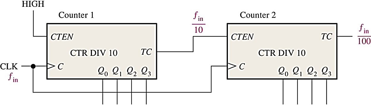
- Cascading means that the last stage output of one counter drives the input stage of the next counter to achieving higher-modulus counters. The following figure shows two asynchronous cascaded counters with an overall modulus of 4 x 8 = 32.
- For synchronous IC counters, the next counter is enabled only when the terminal count (TC) of the previous stage is reached, as shown below:
Decoding Counters #
- Decoding is the detection of a binary number and can be done with an AND gate. A decoding counter which uses an AND gate to decode the decimal number 6 is shown below:

- Notice that when Q0 = 0, Q1 = 1, Q2 = 1 a HIGH appears on the output of the decoding gate, indicating that the counter is at state 6. This is called active-HIGH decoding. Replacing the AND gate with a NAND gate provides active-LOW decoding.
Shift Register #
Basic Shift Register Operations #
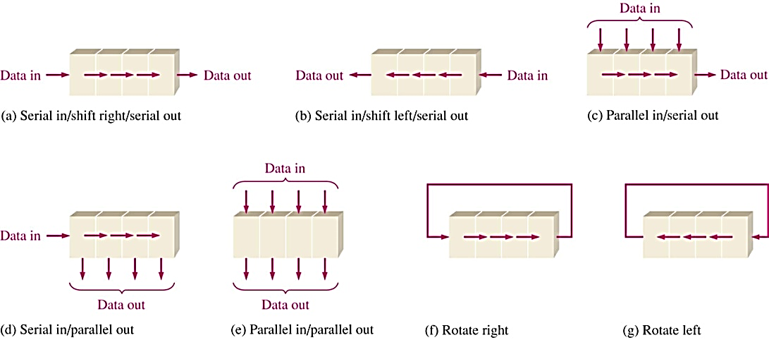
- A shift register is an arrangement of flip-flops with important applications in storage and movement of data. Some basic data movements are illustrated below:
- Serial-In/Serial Out Shift Register: Shift registers are available in IC form or can be constructed from discrete flip-flops. Shown below a five-bit serial-in serial-out register:
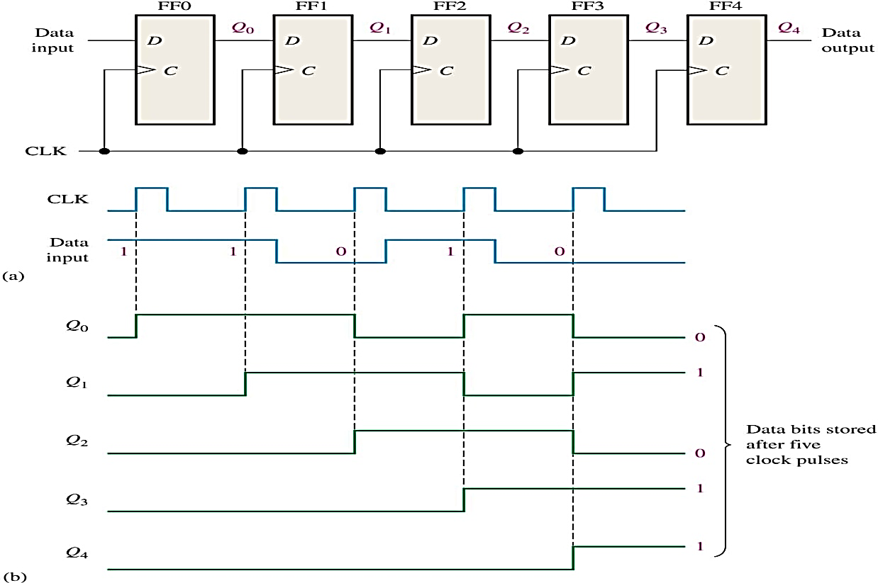
- The LSB ,1, is entered into the register on the 1st clock pulse and then shifted from left to right as the remaining bits are entered and shifted.
- After 5 clock pulses the register contains Q4Q3Q2Q1Q0 = 11010, where the LSB,1, appears on the Q4 output. When the clock pulse 6 is applied, the LSB is shifted out of the shift register and the second bit appears on the Q4 output, and so on until all data are shifted out serially.
5.4.2 Serial-In/Parallel Out Shift Register #
- An application of shift registers is conversion of serial data to parallel form. For example, assume the binary number 0110 is loaded sequentially, one bit at each clock pulse. After 4 clock pulses, the data is available at the parallel output.

Parallel -In/ Serial Out Shift Register #
- Shift registers can be used to convert parallel data to serial form. A logic diagram for this type of register is shown:

- Notice that there are 4 data-input lines, D0, D1, D2, and D3, and a SHIFT/LOAD‘ input, which allows 4 bits of data to load in parallel into the register.
- When SHIFT/LOAD‘ is LOW, gates G1 through G4 are enabled, allowing each data bit to applied to the D input of its respective flip-flop. When a clock pulse is applied, the flip-flops with D=1 will SET and those with D=0 will RESET, thereby storing four bits simultaneously.
- When SHIFT/LOAD‘ is HIGH , gates G1 through G4 are disabled and gates G5 through G7 are enabled, allowing the data bits to shift right from one stage to the next.
Bi-directional Shift Register #
Bidirectional shift registers can shift the data in either direction using a RIGHT/LEFT input.
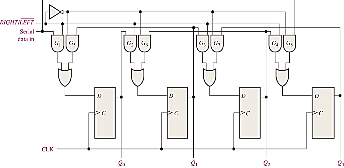
- When the RIGHT/LEFT’ control input is HIGH, gates G1 through G4 are enabled, and the state of the Q output of each flip-flop is passed through to the D input of the following flip-flop. When a clock pulse occurs, the data bits are shifted one place to the right.
- When the RIGHT/LEFT’ control input is LOW, gates G5 through G8 are enabled, and the state of the Q output of each flip-flop is passed through to the D input of the preceding flip-flop. When a clock pulse occurs, the data bits are shifted one place to the left. The output wave forms are shown below

Shift Register Counters #
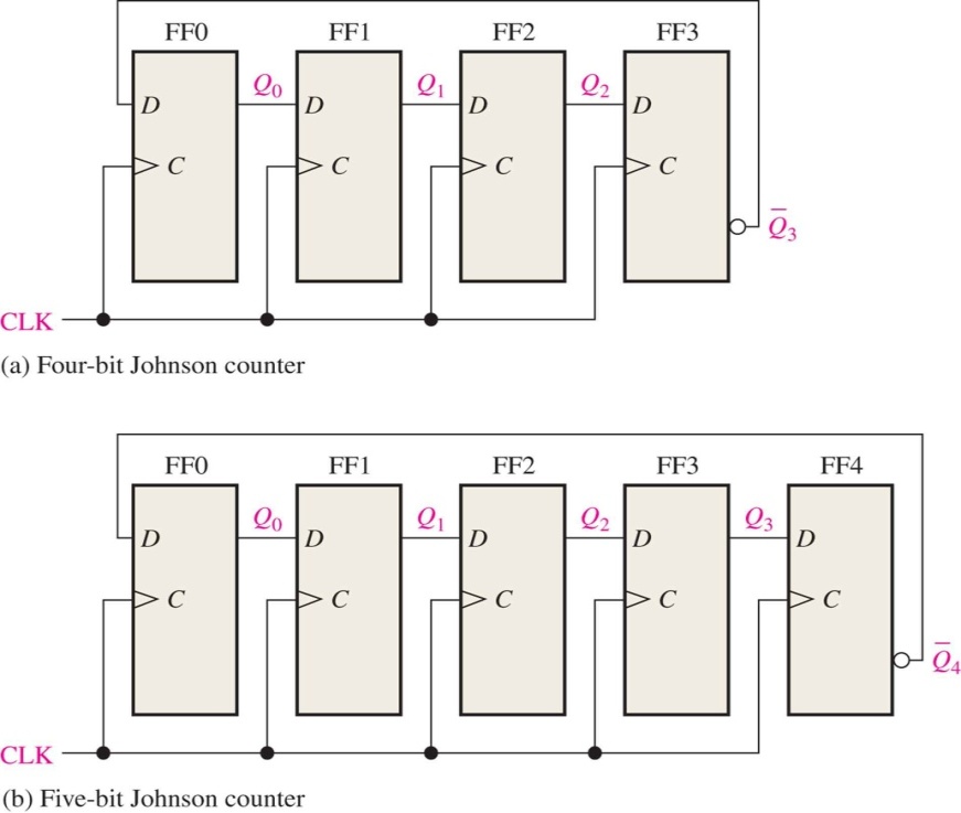
The Johnson Counter #
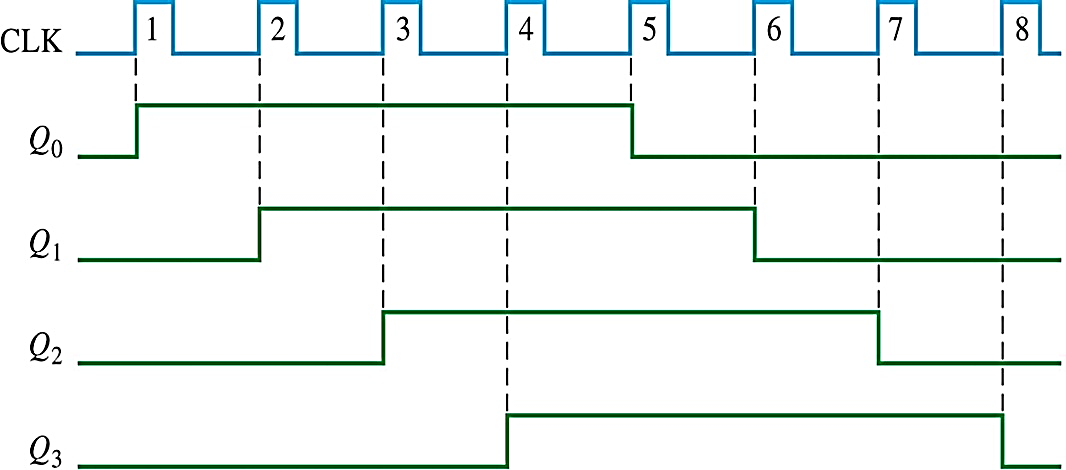
- In a Johnson counter the complement of the output of the last flip-flop is connected back to the D input of the first flip-flop. If the counter starts at 0, this feedback arrangement produces a characteristic sequence of states, as shown in the following table for a 4-bit counter
| Clock pulse | Q0 | Q1 | Q2 | Q3 |
| 0 | 0 | 0 | 0 | 0 |
| 1 | 1 | 0 | 0 | 0 |
| 2 | 1 | 1 | 0 | 0 |
| 3 | 1 | 1 | 1 | 0 |
| 4 | 1 | 1 | 1 | 1 |
| 5 | 0 | 1 | 1 | 1 |
| 6 | 0 | 0 | 1 | 1 |
| 7 | 0 | 0 | 0 | 1 |
- Notice that the 4-bit sequence has a total of 8 states, in general, a Johnson counter will produce a modulus of 2n, where n is the number of stages.
- The implementation of the 4-stage and the 5-stage Johnson counters, along with the timing diagram for the 4-stage counter are shown below
The Ring Counter #
- The ring counter utilizes one flip-flop for each state in its sequence. It has the advantage that decoding gates are not required. In the case of 4-bit ring counter, there is a unique output for each decimal digit. A logic diagram for a 4-bit ring counter and its sequence counts are shown below

| Clock pulse | Q0 | Q1 | Q2 | Q3 | Q4 |
| 0 | 1 | 0 | 0 | 0 | 0 |
| 1 | 0 | 1 | 0 | 0 | 0 |
| 2 | 0 | 0 | 1 | 0 | 0 |
| 3 | 0 | 0 | 0 | 1 | 0 |
| 4 | 0 | 0 | 0 | 0 | 1 |
| 5 | 0 | 0 | 0 | 0 | 0 |
| 6 | 0 | 0 | 0 | 0 | 0 |
| 7 | 0 | 0 | 0 | 0 | 0 |
| 8 | 0 | 0 | 0 | 0 | 0 |
| 9 | 0 | 0 | 0 | 0 | 0 |
Summary #
- Circuits whose outputs depend not only on the present input value but also the past input value are known as sequential logic circuits. It requires memory to store past input
- Synchronous sequential circuits change their states and output values at discrete instants of time, which are specified by the rising and falling edge of a free-running clock signal.
- In asynchronous sequential circuits, the transition from one state to another is initiated by the change in the primary inputs; there is no external synchronization.
Latches and flip flops #
- A bistable multivibrator is one with two stable output states. It can be used to store 1bit data
- In a bistable multivibrator, the condition of Q=1 and Q’=0 is defined as set. A condition of Q=0 and Q’=1 is conversely defined as reset
- In an S-R latch, activation of the S input sets the circuit, while activation of the R input resets the circuit. If both S and R inputs are activated simultaneously, the circuit will be in an invalid condition called race condition.
- A race condition is a state in a sequential system where two mutually-exclusive events are simultaneously initiated by a single cause.
- The gated latch has an additional input, called enable (EN) that must be HIGH in order for the latch to respond to the S and R inputs.
- A D latch is like an S-R latch with only one input: the “D” input. Here S’ is given to R input. Activating the D input sets the circuit, and de-activating the D input resets the circuit. Of course, this is only if the enable input (E) is activated as well. Otherwise, the output(s) will be latched, unresponsive to the state of the D input.
- D latches can be used as 1-bit memory circuits, storing either a “high” or a “low” state when disabled, and “reading” new data from the D input when enabled.
- A flip-flop is a clocked device, which changes state only at clock edge. A flip-flop is a latch circuit with a “pulse detector” circuit connected to the enable (E) input, so that it is enabled only for a brief moment on either the rising or falling edge of a clock pulse.
- Latch are used in asynchronous circuit while flip flops are used in synchronous circuit
- Flip flop can be level or edge triggered which can trigger at positive or negative edge or level.
- Setup time is the time period the input must be held stable before the clock edge occurs.
- Hold time is the time period the input must be held stable after the clock edge occurs.
- In JK flip flop avoids race condition of SR flip flop, where output are feedback to input such that when J=K=1 output toggles
- J and K inputs are combined together to make Toggle (T) flip flop
Counters #
- An “up” counter may be made by connecting the clock inputs of positive-edge triggered J-K flip-flops to the Q’ outputs of the preceding flip-flops. Another way is to use negative-edge triggered flip-flops, connecting the clock inputs to the Q outputs of the preceding flip-flops. In either case, the J and K inputs of all flip-flops are connected to Vcc or Vdd so as to always be “high.”
- Counter circuits made from cascaded J-K flip-flops where each clock input receives its pulses from the output of the previous flip-flop invariably exhibit a ripple effect, Asynchronous counters are sometimes called ripple counters, because the stages do not all change together. It sometime produces glitch i.e. incorrect output for small propagation delay.
- Strobing is a technique applied to circuits receiving the output of an asynchronous (ripple) counter, so that the false counts generated during the ripple time will have no ill effect. Essentially, the enable input of such a circuit is connected to the counter’s clock pulse in such a way that it is enabled only when the counter outputs are not changing, and will be disabled during those periods of changing counter outputs where ripple occurs.
- In synchronous counter all flip-flops are clocked together with a common clock pulse. Synchronous counters overcome the disadvantage of accumulated propagation delays
- Each of the higher-order flip-flops are made ready to toggle (both J and K inputs “high”) if the Q outputs of all previous flip-flops are “high.” Otherwise, the J and K inputs for that flip-flop will both be “low. This can be achieved by ANDing output from previous flip-flops
- Synchronous or asynchronous counter can be truncated to any value like decade counters by making combinational circuit which gives high signal on that value and sending that high signal to clear line.
Shift Register #
- A simple Shift Register can be made using only D-type flip-Flops, one flip-Flop for each data bit.
- The output from each flip-Flop is connected to the D input of the flip-flop at its right.
- Shift registers hold the data in their memory which is moved or “shifted” to their required positions on each clock pulse.
- Each clock pulse shifts the contents of the register one bit position to either the left or the right.
- The data bits can be loaded one bit at a time in a series input (SI) configuration or be loaded simultaneously in a parallel configuration (PI).
- Data may be removed from the register one bit at a time for a series output (SO) or removed all at the same time from a parallel output (PO).
- One application of shift registers is converting between serial and parallel data.
- Shift registers are identified as SIPO, SISO, PISO, PIPO, and universal shift registers.


