
Logic Gates and logic families #
logic gates #
A logic gate is an elementary building block of a digital circuit There are seven basic logic gates: AND, OR, XOR, NOT, NAND, NOR, and XNOR.
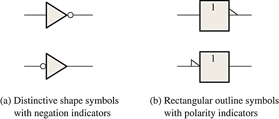
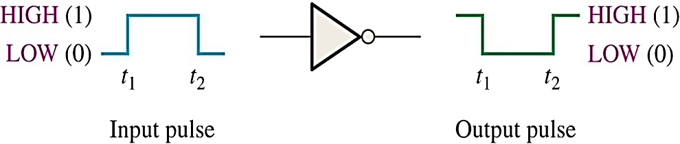
The Inverter #
The inverter performs the Boolean NOT operation. When the input is LOW, the output is HIGH; when the input is HIGH, the output is LOW.
Truth Table
| INPUT (A) | OUTPUT(X) |
| LOW(0) | HIGH(1) |
| HIGH(1) | LOW(0) |
The NOT operation (complement) is shown with an overbar. Thus, the Boolean expression for an inverter is: X = A’
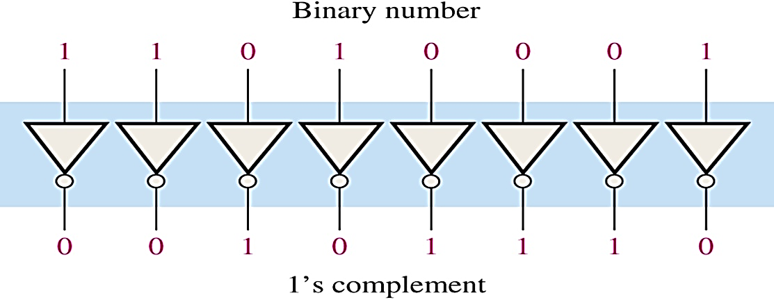
A group of inverters can be used to form the 1’s complement of a binary number:
The AND Gate #
The AND gate produces a HIGH output when all inputs are HIGH; otherwise, the output is LOW.
![]()

(a)Distinctive Shape (b)Rectangular outline with the AND (&) symbol
For a 2-input AND gate, the truth table is:
| INPUTS | OUTPUT | |
| A | B | X |
| 0 | 0 | 0 |
| 0 | 1 | 0 |
| 1 | 0 | 0 |
| 1 | 1 | 1 |
The AND operation is usually shown with a dot between the variables but it may be implied (no dot). Thus, the AND operation is written as:
X = A .B or X = AB
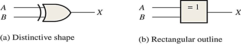
The OR Gate #
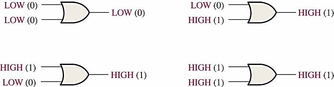
The OR gate produces a HIGH output if any input is HIGH; if all inputs are LOW, the output is LOW. For a 2-input OR gate, the truth table is:
| INPUTS | OUTPUT | |
| A | B | X |
| 0 | 0 | 0 |
| 0 | 1 | 1 |
| 1 | 0 | 1 |
| 1 | 1 | 1 |
The OR operation is shown with a plus sign (+) between the variables. Thus, the OR operation is written as:
X = A + B
Universal Gate #
The NAND Gate #
The NAND gate produces a LOW output when all inputs are HIGH; otherwise, the output is HIGH.
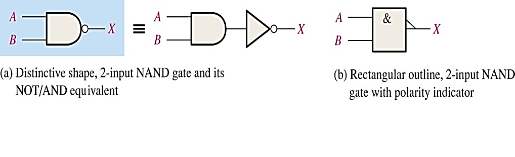
For a 2-input NAND gate, the truth table is:
| INPUTS | OUTPUT | |
| A | B | X |
| 0 | 0 | 1 |
| 0 | 1 | 1 |
| 1 | 0 | 1 |
| 1 | 1 | 0 |
The NAND operation is shown with a dot between the variables and an overbar covering them. Thus, the NAND operation is written as:
X = (A .B)’ or X = (AB)’
The NAND gate is particularly useful because it is a “universal” gate – all other basic gates can be constructed from NAND gates.
Note that
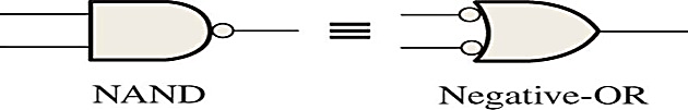
The NAND gate is equivalent to the inverted input (negative) OR gate
The NOR Gate #
The NOR gate produces a LOW output if any input is HIGH; if all inputs are HIGH, the output is LOW.
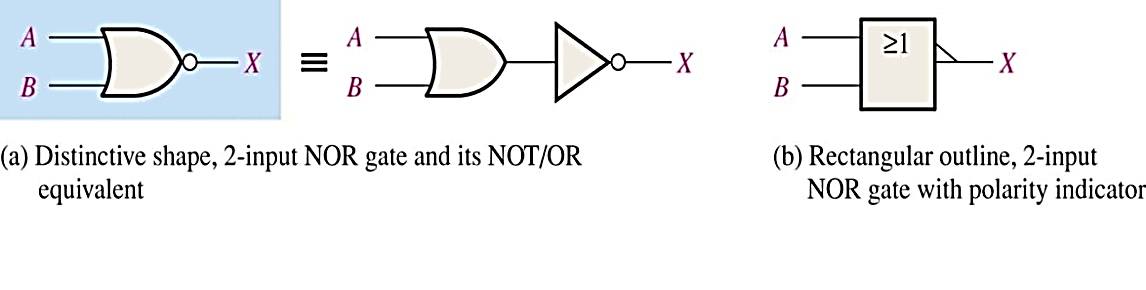
For a 2-input NOR gate, the truth table is:
| INPUTS | OUTPUT | |
| A | B | X |
| 0 | 0 | 1 |
| 0 | 1 | 0 |
| 1 | 0 | 0 |
| 1 | 1 | 0 |
The NOR operation is shown with a plus sign (+) between the variables and an overbar covering them. Thus, the NOR operation is written as:
X = (A + B)’
Note that
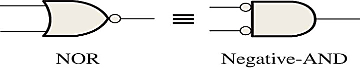
The NOR gate is equivalent to the inverted input (negative) AND gate
2.3 Other Gates
2.3.1 The XOR Gate
The XOR gate produces a HIGH output only when both inputs are at opposite logic levels.
The truth table is:
| INPUTS | OUTPUT | |
| A | B | X |
| 0 | 0 | 0 |
| 0 | 1 | 1 |
| 1 | 0 | 1 |
| 1 | 1 | 0 |
The XOR operation is written as:
X = A’B + AB’
Alternately, it can be written with a circled plus sign between the variables as
The XNOR Gate #
The XNOR gate produces a HIGH output only when both inputs are at the same logic level.

The truth table is:
| INPUTS | OUTPUT | |
| A | B | X |
| 0 | 0 | 1 |
| 0 | 1 | 0 |
| 1 | 0 | 0 |
| 1 | 1 | 1 |
The XNOR operation shown as:
X = A’B’ + AB
Alternately, the XNOR operation can be shown with a circled dot between the variables. Thus, it can be shown as:
Logic families #

Out of all these logic types TTL, MOS, and CMOS are the ones used today.
Diode logic (DL) #
- Diode logic (DL) uses diodes to implement logical functions like AND and OR
- the disadvantage is NOT operation cannot be implemented.
- There was level shifted NOT implemented which was having large offset and low noise margin
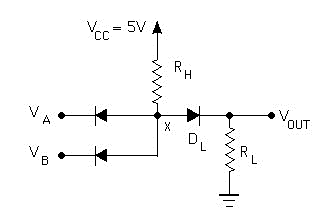
Diode logic AND operation #
 |
With either input at 0V,
Vd=0.7V, and VOUT = 0.7 V. With both inputs at 1 Vd is just cut off, and Vout = +V |
Level-Shifted Diode Logic Two-Input NAND Gate #
 |
With either input at 0V,
Vx=0.7 V, DL is just cut off, and VOUT = 0 V. With both inputs at 1 V, VX=1.7 V and VOUT=1 V. |
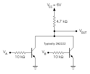
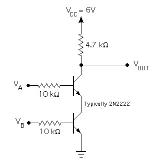
Resistor-transistor logic (RTL) #
- Disadvantage was large space required on IC by resistor
| Two-Input NOR Gate | Two-Input NAND Gate |
 |
 |
Diode-transistor logic (DTL) #
Similar to DL where transistor is used as invertor for two input NAND gate
 |
If all inputs are high, Vbe = + V and the transistor is saturated. If any input goes low Vbe = 0.7 and the transistor may go to cuts off. This circuit have very low nose margin for zero input so two diodes are added at base just to provide 1.4 v drops |
A Diode-Transistor Logic (DTL) Two-Input NAND Gate #
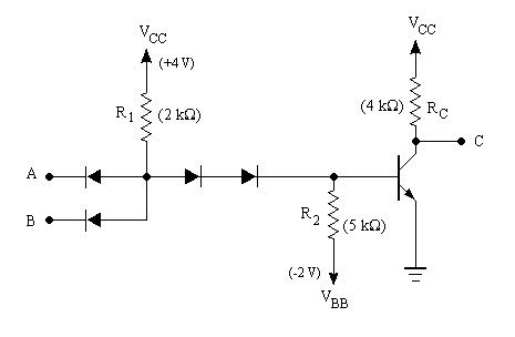 |
If all inputs are high, Vx = 2.2 V the transistor is saturated.
If any input goes low (0.2 V), Vx = 0.9 V and the transistor cuts off. The added resistor R2 provides a discharge path for stored base charge in the BJT, to provide a reasonable L->H transition time. |
Transistor-Transistor Logic (TTL) #
TTL NOT Gate circuit #
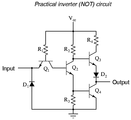
The single-transistor inverter circuit is actually too crude to be of practical use as a gate.
Real inverter circuits contain more than one transistor to maximize voltage gain (so as to ensure that the final output transistor is either in full cutoff or full saturation), and other components designed to reduce the chance of accidental damage.
Practical inverter (NOT) circuit
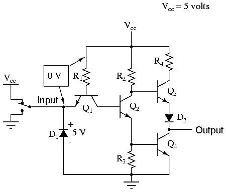
Let’s analyze this circuit for the condition where the input is “high,” or in a binary “1” state. We can simulate this by showing the input terminal connected to Vcc through a switch:
In this case, diode D1 will be reverse-biased, and therefore not conduct any current. In fact, the only purpose for having D1 in the circuit is to prevent transistor damage in the case of a negative voltage being impressed on the input
Transistor Q1 is not being used as is customary for a transistor. In reality, Q1 is being used in this circuit as nothing more than a back-to-back pair of diodes. The purpose of these diodes is to “steer” current to or away from the base of transistor Q2, depending on the logic level of the input.
With base current provided, transistor Q2 will be turned “on.”
more-than-adequate current allowed by R1 through the base. With Q2saturated
Resistor R3 will be dropping enough voltage to forward-bias the base-emitter junction of transistor Q4, thus saturating it as well
With Q4 saturated, the output terminal will be almost directly shorted to ground, leaving the output terminal at a voltage binary “0” (“low”) logic level.
Due to the presence of diode D2, there will not be enough voltage between the base of Q3 and its emitter to turn it on, so it remains in cutoff.
if we reverse the input’s logic level to a binary “0” by actuating the input switch
there will be current through the left steering diode of Q1 and no current through the right steering diode.
This eliminates current through the base of Q2, thus turning it off. With Q2off, there is no longer a path for Q4 base current, so Q4 goes into cutoff as well.
Q3, on the other hand, now has sufficient voltage dropped between its base and ground to forward-bias its base-emitter junction and saturate it, thus raising the output terminal voltage to a “high” state.
In actuality, the output voltage will be somewhere around 4 volts depending on the degree of saturation and any load current, but still high enough to be considered a “high” (1) logic level.
Current sourcing and sinking: #
Simplified gate circuit sourcing current
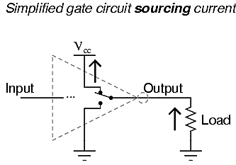
The combination of Q3 and Q4 working as a “push-pull” transistor pair (otherwise known as a totem pole output) has the ability to either source current (draw in current to Vcc) or sink current (output current from ground) to a load.
However, a standard TTL gate input never needs current to be sourced, only sink. That is, since a TTL gate input naturally assumes a high state if left floating, any gate output driving a TTL input need only sink current to provide a “0” or “low” input, and need not source current to provide a “1” or a “high” logic level at the input of the receiving gate:
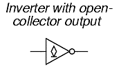
This means we have the option of simplifying the output stage of a gate circuit so as to eliminate Q3 altogether. The result is known as an open-collector output:
Inverter circuit with open – collector output
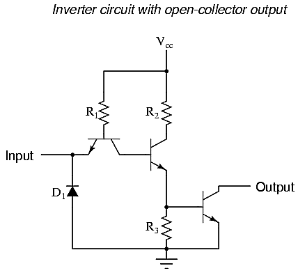
To designate open-collector output circuitry within a standard gate symbol, a special marker is used. Shown here is the symbol for an inverter gate with open-collector output:
Please keep in mind that the “high” default condition of a floating gate input is only true for TTL circuitry, and not necessarily for other types, especially for logic gates constructed of field-effect transistors.
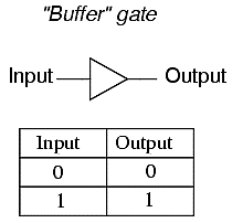
The “Buffer” gate #
If we were to connect two inverter gates together so that the output of one fed into the input of another, the two inversion functions would “cancel” each other out so that there would be no inversion from input to final output:

While this may seem like a pointless thing to do, it does have practical application. Remember that gate circuits are signal amplifiers, regardless of what logic function they may perform. A weak signal source (one that is not capable of sourcing or sinking very much current to a load) may be boosted by means of two inverters like the pair shown in the previous illustration. The logic level is unchanged, but the full current-sourcing or -sinking capabilities of the final inverter are available to drive a load resistance if needed.
For this purpose, a special logic gate called a buffer is manufactured to perform the same function as two inverters. Its symbol is simply a triangle, with no inverting “bubble” on the output terminal:
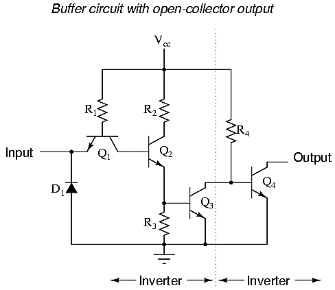
The internal schematic diagram for a typical open-collector buffer is not much different from that of a simple inverter: only one more common-emitter transistor stage is added to re-invert the output signal.
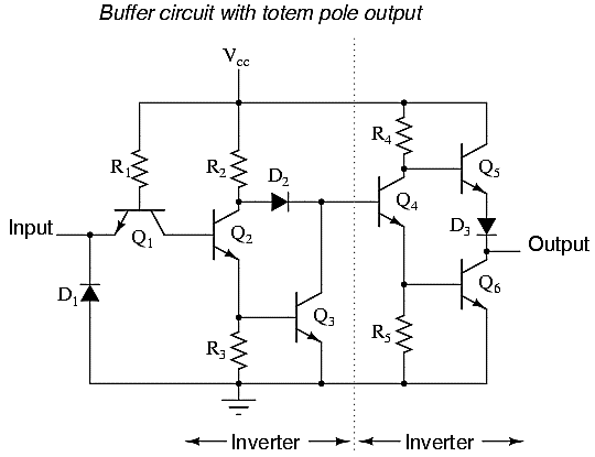
Basic Multi-emitter TTL Three-Input NAND Gate #
 |
All Inputs High
– QI is reverse active. – QO is saturated. – VOL = VCES Any Input Low – QI is saturated. – QO is cut off. – VOH = VCC Multi-emitter transistor. Forward-biased emitter base junctions override reverse-biased junctions in determining the base and collector currents. |
2.7.5 Advanced TTL Designs #
Schottky Clamping: QS and QO may be Schottky clamped, preventing saturation. This greatly improves TPLH.
Darlington Pull-up: The Darlington pull-up arrangement increases the average output drive current for charging a capacitive load. Although RCP limits the maximum output current, this maximum drive is maintained over a wider range of VOUT than with a single pull-up transistor.
Squaring Circuit: Active pull-down for the base of the output transistor squares the VTC. This will improve the low noise margin. An added benefit is faster charge removal for the output transistor.
Improved Fabrication: Smaller devices, and oxide isolation, have steadily reduced parasitic capacitances and reduced RC time constants.
Darlington Pull-up #
| QP2 is added, forming a Darlington pair with QP.
The EB junction of QP2 introduces a 0.7V level shift, so DL can be eliminated. QP2 cannot saturate, so Schottky clamping is not necessary. REP is needed to provide a discharge path for QP2 base charge. |
The Darlington emitter follower provides a very low output impedance, approaching . This greatly reduces the rise time.
Squaring Circuit #
 |
– There is no path for Qs emitter current unitl QO turn on.
– QS and QO begin to conduct simulta- neously. – BP1 is eliminated from the VTC; in other words, the VTC is “squared.” – VIL is increased, improving the low noise margin. |
In TTL logic gate family three different types of output configurations are available; they are open collector output type, totem-pole output type and tri-state output type.
The speed power product has the units of energy and is expressed in picojoules.
A TTL circuit acts as a current sink in the LOW state and as a current source in the HIGH state.
The TTL is the fastest of all saturated logic families. It is used in SSI and MSI ICs.
Low power TTL uses large resistors to reduce the power requirements, which consequently reduces its speed of operation.
High speed TTL uses smaller resistors and a Darlington pair in place of Q3 to increase its speed.
The speed of Schottky TTL is higher than that of standard TTL, because in Schottky TTL the transistors are not allowed to go into saturation by connecting a Schottky barrier diode between the base and the collector of each transistor.
The totem – pole configuration has the advantages of high speed and low power dissipation but the disadvantages are those of generation of current spikes and the inability to be wire ANDed.
A tri-state gate has three states – HIGH, LOW and HIGH IMPEDANCE state. It utilizes the advantages of high speed of operation of the totem-pole configuration and wire ANDing of the open-collector configuration.
The IIL has the highest packing density and is mainly suitable for VLSI and ULSI.
The ECL is the fastest of all logic families and is mainly used in supercomputers. It is a non-saturated logic. Its logic levels are negative and complementary outputs are available as well.
ECL gates, which are available in open-emitter configuration, can be wired OR.
2.8 CMOS Logic #
CMOS (complementary metal-oxide-semiconductor) technology is used predominantly to create digital circuitry.
The fundamental building blocks of CMOS circuits are P-type and N-type MOSFET transistors.
A P-type MOSFET can be modeled as a switch that is closed when the input voltage is low (0 V) and open when the input voltage is high (5 V).
A N-type MOSFET can be modeled as a switch that is closed when the input voltage is high (5 V) and open when the input voltage is low (0 V).
The basic idea for CMOS technology is to combine P-type and N-type MOSFETs such that there is never a conducting path from the supply voltage (5 V) to ground.
As a consequence, CMOS circuits consume very little energy.

P-type MOSFET : “Switch is closed” when input is 0V.

N-type MOSFET : “Switch is closed” when input is 5V.
CMOS invertor #
When a low voltage (0 V) is applied at the input, the top transistor (P-type) is conducting (switch closed) while the bottom transistor behaves like an open circuit. Therefore, the supply voltage (5 V) appears at the output.
Conversely, when a high voltage (5 V) is applied at the input, the bottom transistor (N-type) is conducting (switch closed) while the top transistor behaves like an open circuit. Hence, the output voltage is low (0 V).
The function of this gate can be summarized by the following table:
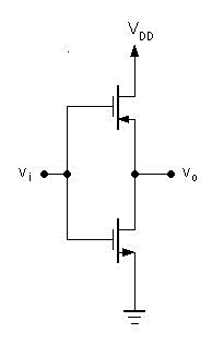
| Input | Output |
| High | Low |
| Low | High |
The output is the opposite of the input – this gate inverts the input.
Notice that always one of the transistor will be an open circuit and no current flows from the supply voltage to ground.
CMOS Two-Input NAND Gate #
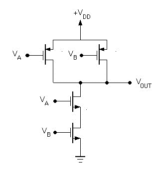
The circuit above has two inputs and one output. Whenever at least one of the inputs is low, the corresponding P-type transistor will be conducting while the N-type transistor will be closed. Consequently, the output voltage will be high.
Conversely, if both inputs are high, then both P-type transistors at the top will be open circuits and both N-type transistors will be conducting. Hence, the output voltage is low.
The function of this gate can be summarized by the following table:
| Va | Vb | Output |
| Low | Low | High |
| Low | High | High |
| High | Low | High |
| High | High | Low |
If logical 1’s are associated with high voltages then the function of this gate is called NAND for negated AND.
Again, there is never a conducting path from the supply voltage to ground.
NOR Gate #
The circuit below has two inputs and one output. Whenever at least one of the inputs is high, the corresponding N-type transistor will be closed while the P-type transistor will be open. Consequently, the output voltage will be low.
Conversely, if both inputs are low, then both P-type transistors at the top will be closed circuits and the N-type transistors will be open.
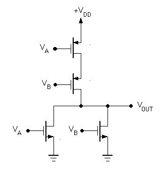
Hence, the output voltage is high.
The function of this gate can be summarized by the following table:
| VA | VB | Output |
| Low | Low | High |
| Low | High | Low |
| High | Low | Low |
| High | High | Low |
If logical 1’s are associated with high voltages then the function of this gate is called NOR for negated OR.
Again, there is never a conducting path from the supply voltage to ground.
The MOS logic is the simplest to fabricate.
A MOS transistor can be connected as a resistor.
Most modern MOSFET circuitry is constructed using NMOS devices because they are three times faster and two times denser than their PMOS counter parts.
The MOS is ideally suited for LSI/VLSI/ULSI and for dedicated applications such as large memories, large microprocessor chips, etc.
The CMOS uses both n-channel and p-channel MOSFETs in the same circuit.
The CMOS requires the least power, whereas ECL requires the maximum power.
The advantages of open-collector output type are wired-logic can be performed and loads other than the normal gates can be used.
The tri-state logic devices are used in bus oriented systems.
If any input of TTL circuit is left floating, it will function as it is connected to logic 1 level.
The supply voltage range of 74 – series is 5 0.25 V and for 54 – series is 5 0.5 V.
Negative supply is preferred in ECL family because the effect of noise present in the supply line is reduced considerably and accidental short-circuiting of output to ground will not damage the gate.
MOS logic is mainly used for LSI and VLSI applications because the silicon chip area required for fabrication of a MOS device is very small.
The fan-out of MOS logic gates is very high because of their high input impedance.
If any unused input terminal of a MOS gate is left unconnected, a large voltage may get induced at the unconnected input which may damage the gate.
Different versions available in TTL logic gate family are given below:
74/54 L : Low power
74/54 H : High-power/ High-speed
74/54 LS : Low-power Schottky
74/54 S : Schottky
74/54 AS : Advanced Schottky
74/54 ALS : Advanced Low-power Schottky
Logic Families Summery #
Comparison of different logic gate families: #
| Property/ Family | DTL | TTL | ECL | CMOS | p-MOS |
| Fan-out | 8 | 10 | 25 | 50 | 20 |
| Propagation Delay | 30 n sec. | 10 n sec. | 4 n sec. | 70 n sec. | 300 n sec. |
| Power Dissipation | 8m W | 10m W | 40m W | 0.01m W | 0-10m W |
| Noise Margin (min.) | 700 mV | 400 mV | 200 mV | 800 mV | 150 mV |
Fastest logic gate family is ECL. It is also called Current Mode Logic.
ECL has high speed and high power consumption.
Slowest logic gate family is CMOS.
The logic gate family, which consumes less power is CMOS.
CMOS has highest noise margin.
The logic gate family, having highest fan out is CMOS.
NMOS is faster than PMOS.
In tri-state logic, in addition to two low impedance Output 0 and 1, there is third output state known has high impedance state.
Characteristic Parameters of logic families #
HIGH-level input current, IIH (current flowing into (taken as positive) or out of (taken as negative) an input when a HIGH-level input voltage equal to the minimum HIGH-level output voltage specified for the family is applied.
LOW-level input current, IIL. is the maximum current flowing into (taken as positive) or out of (taken as negative) the input of a logic function when the voltage applied at the input equals the maximum LOW-level output voltage specified for the family.
unit load (UL) HIGH-level and LOW-level input current or loading typically found in data sheets (For devices of the TTL family, 1 UL (HIGH)=40 A and 1 UL (LOW)=1.6 mA.
HIGH-level output current, IOH. This is the maximum current flowing out of an output when the input conditions are such that the output is in the logic HIGH state. Typically negative number.
LOW-level output current, IOL. This is the maximum current flowing into the output pin of a logic function when the input conditions are such that the output is in the logic LOW state.
HIGH-level off-state (high-impedance state) output current, IOZH. This is the current flowing into an output of a tristate logic function with the ENABLE input chosen so as to establish a high-impedance state and a logic HIGH voltage level applied at the output. The input conditions are chosen so as to produce logic LOW if the device is enabled.


LOW-level input voltage, VIL. This is the maximum voltage level applied at the input that is recognized as a legal LOW level for the specified family.
HIGH-level output voltage, VOH. This is the minimum voltage on the output pin of a logic function when the input conditions establish logic HIGH at the output for the specified family.
HIGH-level output voltage, VOH. This is the minimum voltage on the output pin of a logic function when the input conditions establish logic HIGH at the output for the specified family.

Supply current, ICC. The supply current when the output is HIGH, LOW and in the high-impedance state is respectively designated as ICCH, ICCL and ICCZ.
Rise time, tr. This is the time that elapses between 10 and 90 % of the final signal level when the signal is making a transition from logic LOW to logic HIGH.
Fall time, tf . This is the time that elapses between 90 and 10 % of the signal level when it is making HIGH to LOW transition
Propagation delay tp. is the time delay between the occurrence of change in the logical level at the input and before it is reflected at the output. It is the time delay between the specified voltage points on the input and output waveforms.
Propagation delays are separately defined for LOW-to-HIGH and HIGH-to-LOW transitions at the output. In addition, we also define enable and disable time delays that occur during transition between the high-impedance state and defined logic LOW or HIGH states.
For positive logic system

For negative logic system

Maximum clock frequency, fmax. This is the maximum frequency at which the clock input of a flip-flop can be driven through its required sequence while maintaining stable transitions of logic level at the output in accordance with the input conditions and the product specification.
Power dissipation. The power dissipation parameter for a logic family is specified in terms of power consumption per gate and is the product of supply voltage VCC and supply current ICC.
ICC : Average supply current
ICCH : Current value when output is high
ICCL : Current value when output is low
Speed–power product. The speed of a logic circuit can be increased, that is, the propagation delay can be reduced, at the expense of power dissipation.
Fan-out. is the number of inputs of a logic function that can be driven from a single output without causing any false output.
Noise margin. This is a quantitative measure of noise immunity offered by the logic family. When the output of a logic device feeds the input of another device of the same family, a legal HIGH logic state at the output of the feeding device should be treated as a legal HIGH logic state by the input of the device being fed. Similarly, a legal LOW logic state of the feeding device should be treated as a legal LOW logic state by the device being fed.
called high level noise margin
called low level noise margin

Summary: #
Summary
| Logic Family | Advantages | Disadvantages |
| RTL | Low power dissipation. | 1. Insufficient noise margins.
2. Low speed. |
| DTL | Low power dissipation. | 1. Poor noise margins.
2. Low speed. |
| TTL | 1. Low power dissipation.
2. High speed. 3. High fan-out capability. 4. High compatibility with existing systems. 5. Low cost. |
1. Light VCC tolerance.
2. Susceptible to power translents. |
| ECL | 1. Very high speed.
2. High fan out capability. 3. Low noise generation. 4. Complementary output. |
1. Difficult to iterance with other logic families.
2. High cost. 3. Requiring careful circuit layout. |
| MOS | 1. Increased circuit complexity per package.
2. Low cost per circuit function. 3. Fewer parts to assemble and inspect. 4. Lower power drain per function. |
1. Very low speed.
2. Requiring multiple power sources to property operate and interface to other logic families. |
| CMOS | 1. Extremely low power consumption when operated at low speed.
2. Relative Insensitive to variations in VDD. 3. High noise immunity. 4. Compatible (through. appropriate buffers) to most existing logic families. |
1. Low speed.
2. Susceptible to static discharge damage. |
| IIL | 1. Speed-power product constant and low.
2. Very high packing density. |


