
Combinational Logic Analysis #
- When logic gates are connected together to produce a specified output for certain specified combination of input variables, with no storage involved, the resulting circuit is in the category of combinational logic.
- In combinational logic, the output level is at all times dependent on the combination of input levels.
Implementation of Boolean Logic #
Exclusive-OR Logic #
The output of an Exclusive-OR gate is HIGH whenever its inputs A and B are different, its logic diagram and symbol is illustrated below:
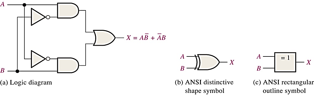
The XOR operation is written as:
X = AB’+ A’B or as
Exclusive-NOR Logic #
The output of an Exclusive-OR gate is HIGH whenever its inputs A and B are the same, its logic diagram is illustrated below:
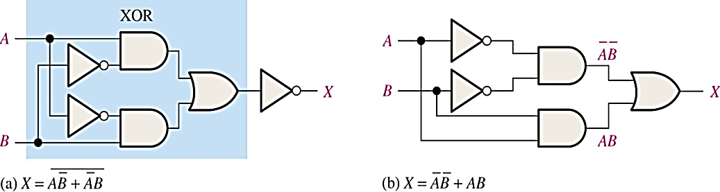
The XNOR operation is written as:
X = A’B’+ AB or as
From a Boolean Expression to a Logic Circuit #
To implement the Boolean expression: X = AB (CD’ + EF)
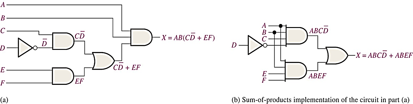
Notice that, in part (b), the same circuit is implemented for the SOP expression. The second circuit has fewer gates as well as less propagation delay.
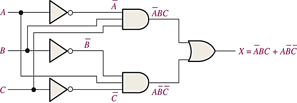
From a Truth Table to a Logic Circuit #
If you begin with a truth table instead of an expression, you can write the SOP expression from the truth table and then implement the circuit, as follows:
| A B C | X | PRODUCT TERM |
| 0 0 0 | 0 | |
| 0 0 1 | 0 | |
| 0 1 0 | 0 | |
| 0 1 1 | 1 | A’BC |
| 1 0 0 | 1 | AB’C’ |
| 1 0 1 | 0 | |
| 1 1 0 | 0 | |
| 1 1 1 | 0 |
The Boolean SOP expression obtained from the truth table by ORing the product terms for which X=1 is: X = A‘BC + AB‘C‘
The logic gates required to implement this expression are as follows:
Universal Gates #
NAND gates are sometimes called universal gates because they can be used to produce the other basic Boolean functions.
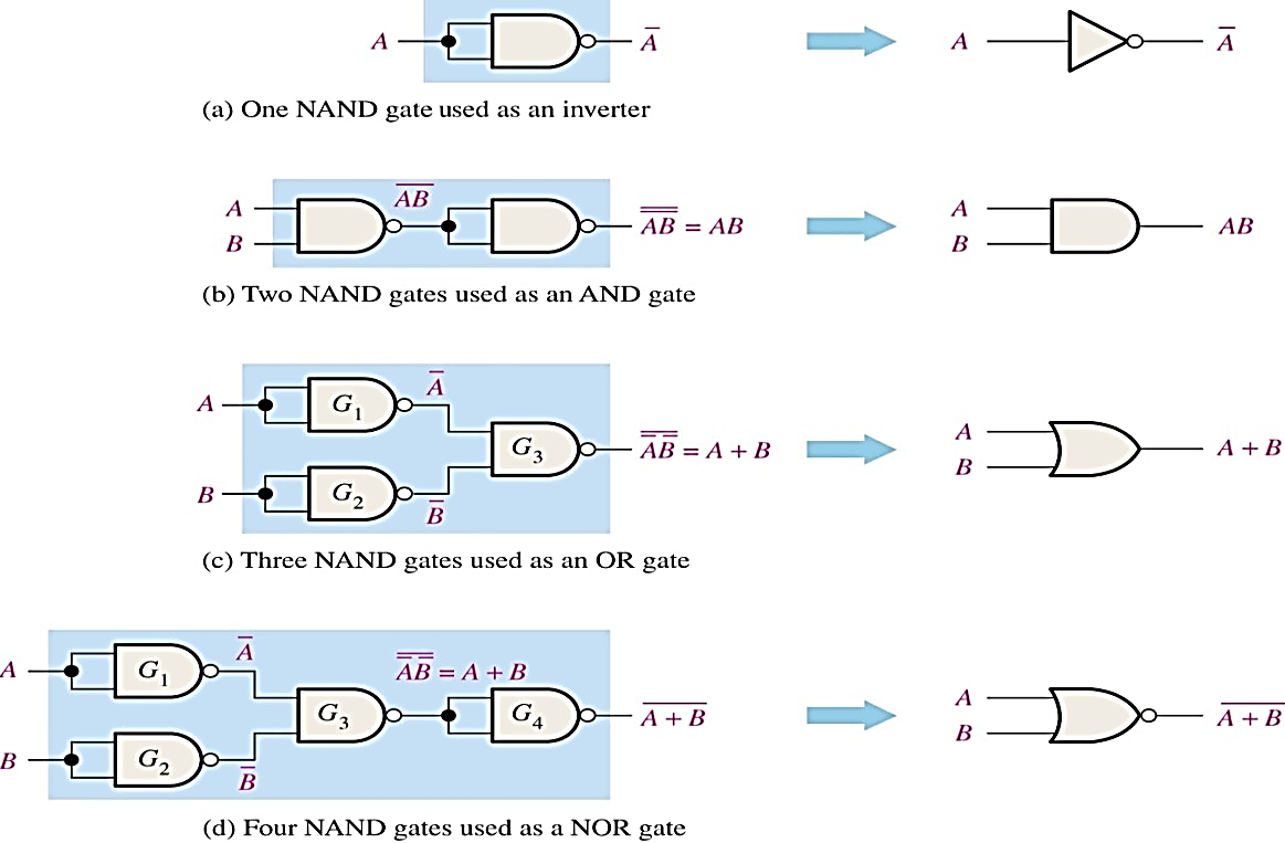
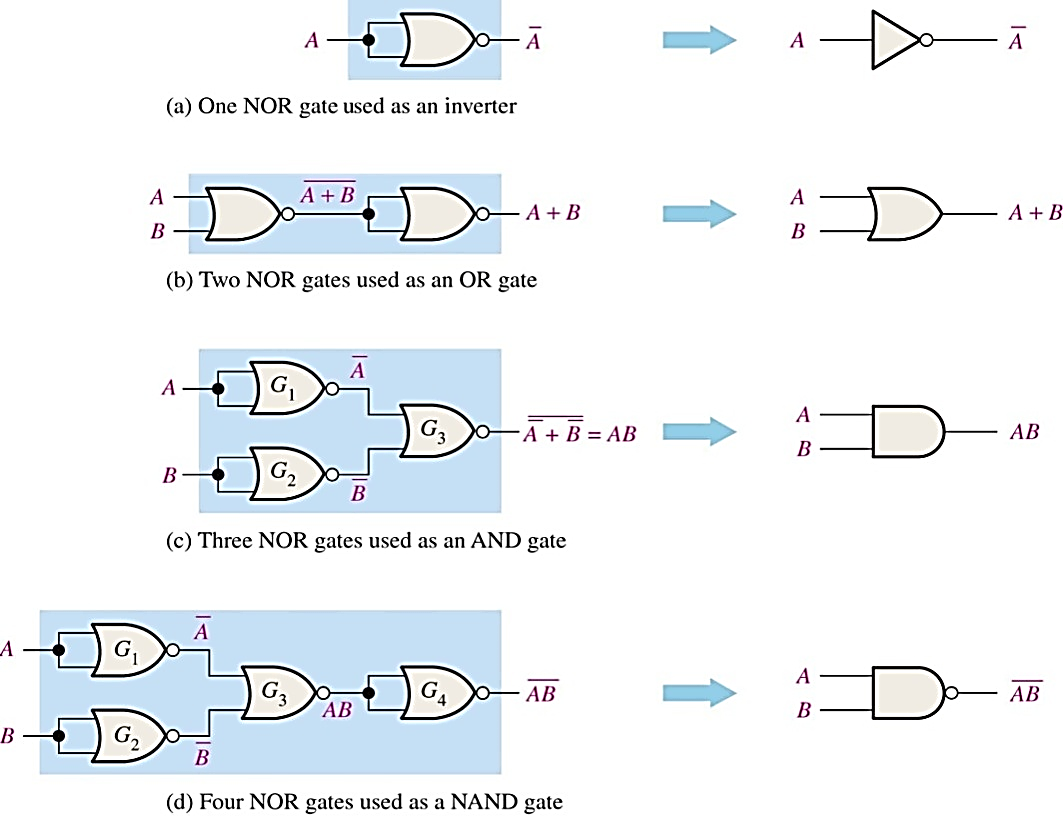
NOR gates are also universal gates and can form all of the basic gates.
- Minimum number of NAND gate required to realize X-NOR gate is 5.

- Minimum number of NOR gate required to realize X-NOR gate is 4.

- Minimum number of NOR gate required to realize X-OR gate is 5.
Combinational Logic Using Universal Gates #
- To implement NAND logic converts expression in to SOP form
- To implement NOR logic converts expression in to POS form
Pulsed Waveforms #
For combinational circuits with pulsed inputs, the output can be predicted by developing intermediate outputs and combining the result. For example, the circuit shown below can be analyzed at the outputs of the AND gates:

Determining the intermediate outputs of gates G2 and G3, the resulting “final” output can be derived, as follows:
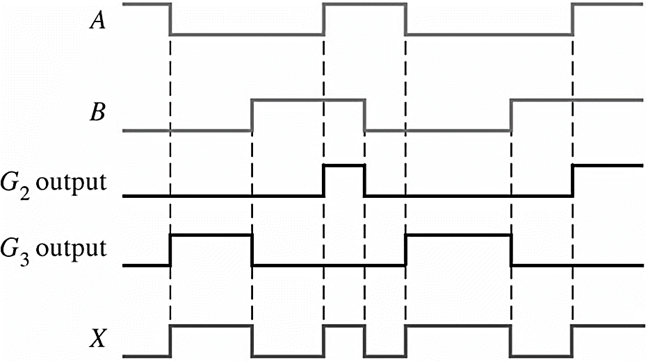
When the primary inputs A and B are the same (HIGH or LOW), the output X is HIGH. Thus the circuit is equivalent to an XNOR gate.
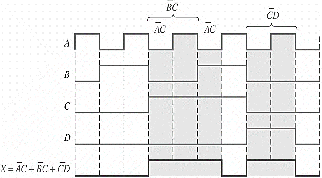
Alternately, you can determine the output waveform directly by developing the SOP expression as in the following example.
Example: Determine the output waveform X for the given circuit by developing the output SOP expression.

Solution: The output SOP expression X = A’C + B’C + C’D indicates that the output X is HIGH when: A is LOW and C is HIGH, or B is LOW and C is HIGH, or C is LOW and D is HIGH, as shown below:
Adders #
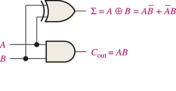
The Half-Adder #
Basic rules of binary addition are performed by a half adder, which has two binary inputs (A and B) and two binary outputs (Carry out and Sum). The inputs and outputs can be summarized on a truth table.
| INPUTS | OUTPUTS | ||
| A | B | ∑ | Cout |
| 0 | 0 | 0 | 0 |
| 0 | 1 | 1 | 0 |
| 1 | 0 | 1 | 0 |
| 1 | 1 | 0 | 1 |
Where:
∑ = Sum, Cout= output carry, A and B = input variables (operands)
Observe that:
The sum output (∑) is a 1 only if the input variables, A and B, are not equal. The sum can therefore be expressed as
the exclusive–OR of the input variables.
∑ = A + B
The output carry (Cout) is a 1 only when both A and B are 1s. Thus Cout can be expressed as the AND of the two input variables.
Cout = AB
The logic symbol and equivalent circuit are:

The Full-Adder #
By contrast, a full adder has three binary inputs (A, B, and Carry in) and two binary outputs (Carry out and Sum).
The truth table summarizes the operation
| INPUTS | OUTPUTS | |||
| A | B | Cin | ∑ | Cout |
| 0 | 0 | 0 | 0 | 0 |
| 0 | 0 | 1 | 1 | 0 |
| 0 | 1 | 0 | 1 | 0 |
| 0 | 1 | 1 | 0 | 1 |
| 1 | 0 | 0 | 1 | 0 |
| 1 | 0 | 1 | 0 | 1 |
| 1 | 1 | 0 | 0 | 1 |
| 1 | 1 | 1 | 1 | 1 |
A full-adder can be constructed from two half adders as shown:

Notice that there are two half-adders connected with their output carries ORed.
The equation of the sum (∑) output of the full adder is:
∑ = (A B)+Cin
The equation of the final output carry Cout of the full adder is:
Cout = AB + (A B) Cin
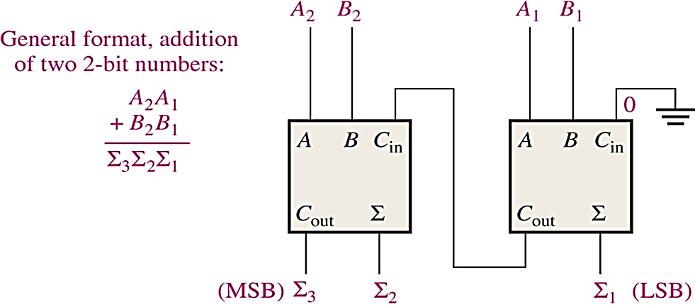
Parallel Binary Adders #
- Two or more full-adders are connected to form binary adders. To add two binary numbers, a full-adder is required for each bit in the number. So for 2-bit numbers, two adders are needed, for 4-bit numbers, four adders are used, and so on.
The carry output of each adder is connected to the carry input of the next higher-order adder as shown below:
Notice that:
- Either a half-adder can be used for the least significant position or the carry input (Cin) of a full-adder can be made 0 (grounded) because there is no carry input to the least significant bit (LSB) position.
- The LSB of the two numbers are represented by A1 and B1. The next higher-order bits are represented by A2 and B2.The three sum bits are ∑1, ∑2, and ∑3. The output carry from the left-most full-adder becomes the MSB in the sum, ∑3.
4 bit The Ripple Carry Adder #
- A ripple carry adder is one in which the carry output of each full-adder is connected to the carry input of the next higher-order stage. The sum and output carry of any stage cannot be produced until the input carry occurs; this causes a time delay in the addition process, as shown below:
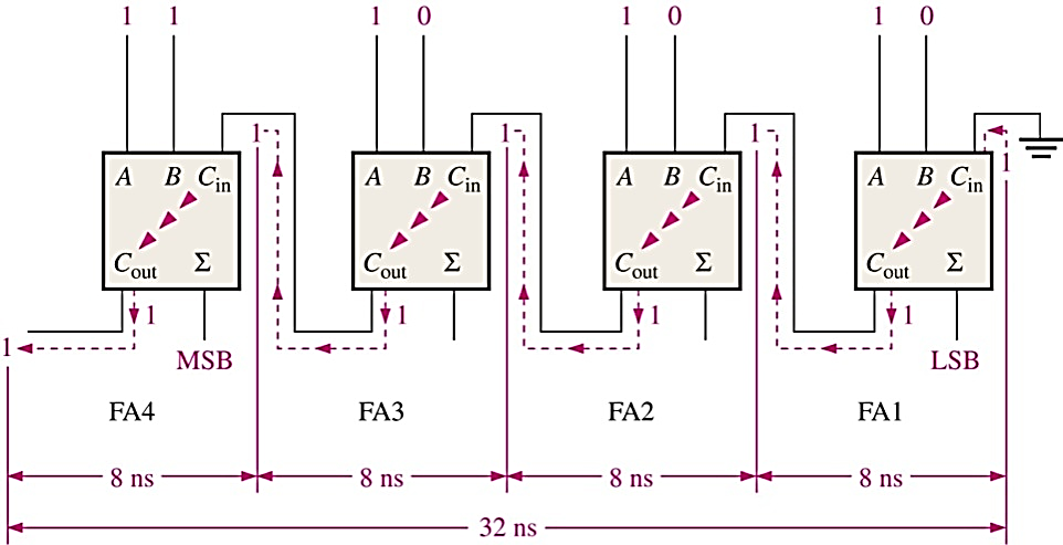
- The carry propagation delay for each full-adder is the time from the application of the input carry, until the output carry occurs. The input carry to the least significant stage has to ripple through all adders before a final sum is produced.
- The cumulative delay through all adder stages is a “worst-case” addition time. If two numbers are added such that no carries (0) occur between stages, the addition time is simply the propagation time through a single full-adder; however, worst-case addition time must always assumed.
The Look-Ahead Carry Adder #
- One method of speeding up the addition process by eliminating this carry delay is called look-ahead carry addition. The look-ahead carry adder anticipates the output carry of each stage, and based on the inputs, produces the output carry by either carry generation or carry propagation.
Carry generation: occurs when an output carry is produces internally by the full-adder. A carry generated only when both inputs are 1s.The generated carry, Cg, is expressed as the AND function of the two input bits, A and B.
Cg = AB
The output carry of a full-adder (Cout) can be expressed in terms of both (Cg) and (Cp) as follows: Cout = Cg + Cp Cin
Thus, Cout = 1 if (Cg = 1) OR if (Cp = 1 AND Cin = 1)
For a 4-bit parallel adder, the output carry for each full-adder stage is dependent only on the initial input carry Cin1, the Cg and Cp functions of that stage, and the Cg and Cp functions of the preceding stages.
Since each of Cg and Cp functions can be expressed in terms of the A and B inputs to the full-adder, all the output carries are immediately available (except for gate delays), and you do not have to wait for a carry to ripple through all stages before a final result is achieved. Thus, the look-ahead carry technique speeds up the addition process.
The Cout equations are implemented with logic gates and connected to the full-adders to create a 4-bit look-ahead carry adder, as shown below:

Comparators #
The function of a comparator is to compare the magnitudes of two binary numbers to determine the relationship between them.
Equality #
In the simplest form, a comparator can test for equality using XNOR gates.
Example: Apply each of the following sets of binary numbers to the comparator inputs shown below, and determine the output by following the logic levels through the circuit. (a) 10 and 10 (b) 11 and 10
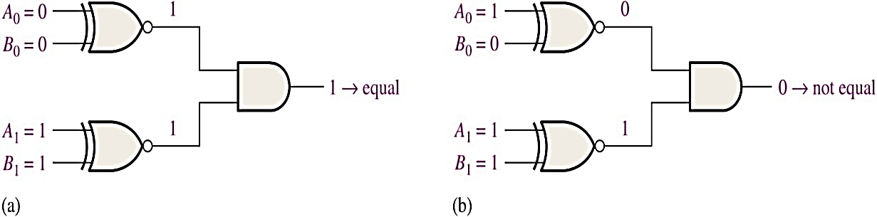
Solution: (a) The output is 1 (equal) for inputs 10 and 10
(b) The output is 0 (not equal) for inputs 11 and 10
Inequality #
In addition to the equality output, many IC comparator, such as 74LS85, provide outputs that indicate when number A is greater than number B (A>B), and when number A is less than number B (A<B), as shown in the logic symbol for a 4-bit comparator below:
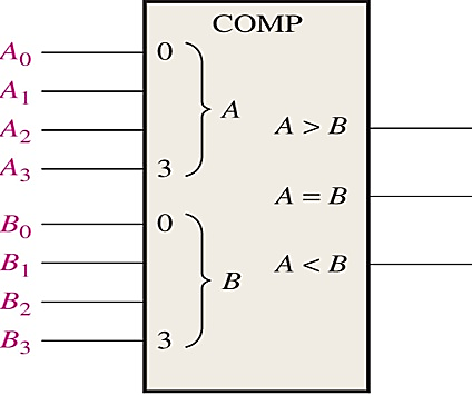
To determine an inequality of binary numbers A and B, you first examine the highest-order bit in each number. The following conditions are possible:
If A3 = 1 and B3 = 0, number A is greater than number B.
If A3 = 0 and B3 = 1, number A is less than number B.
If A3 = B3, then you must examine the next lower bit position for an inequality.
Decoder:
A decoder is a logic circuit that converts an n-bit binary code into (2n) output lines such that each output line will be activated for only one of the possible combinations of inputs.
Decoders are available in two different types of output forms:
1. Active high output type decoders and
2. Active low output type of decoders.
Active high output type decoders are constructed with AND gates and active low output type of decoders are constructed with NAND gates.
A decoder with enable input acts as de-multiplexer.
Truth table of active high output type of decoder:
| X | Y | D0 | D1 | D2 | D3 |
| 0 | 0 | 1 | 0 | 0 | 0 |
| 0 | 1 | 0 | 1 | 0 | 0 |
| 1 | 0 | 0 | 0 | 1 | 0 |
| 1 | 1 | 0 | 0 | 0 | 1 |


Active low output type decoders will give the output low for given input combination and all other outputs are high.
| X | Y | D0 | D1 | D2 | D3 |
| 0 | 0 | 0 | 1 | 1 | 1 |
| 0 | 1 | 1 | 0 | 1 | 1 |
| 1 | 0 | 1 | 1 | 0 | 1 |
| 1 | 1 | 1 | 1 | 1 | 0 |

Example: Realization of full-adder using two 3 × 8 decoders.
Sol. S0 = f(A, B, C) =
C0 = f(A, B, C) =

Example: Realization of 4 × 16 decoder using 3 × 8 decoder

Encoders #
The encoder is a combinational logic circuit that essentially performs a “reverse” decoder function. An encoder accepts an active logic level on one of its inputs and converts it to a coded output, such as BCD or binary. In general, the process of converting from familiar symbols or numbers to a coded format is called encoding.
Decimal-to-BCD Encoder #
This type of encoder has ten inputs, one for each decimal digit, and four outputs corresponding to the BCD code, this is a basic 10-lines-to-4-lines encoder, as illustrated below:

The BCD (8421) code is listed in the following table:
| Decimal Digit | BCD Code
A3 A2 A1 A0 |
| 0 | 0 0 0 0 |
| 1 | 0 0 0 1 |
| 2 | 0 0 1 0 |
| 3 | 0 0 1 1 |
| 4 | 0 1 0 0 |
| 5 | 0 1 0 1 |
| 6 | 0 1 1 0 |
| 7 | 0 1 1 1 |
| 8 | 1 0 0 0 |
| 9 | 1 0 0 1 |
From this table you can determine the following logic expressions:
A3 = 8+9 (Bit A3 is always 1 for decimal digit 8, or 9)
A2 = 4+5+6+7 (Bit A2 is always 1 for decimal digit 4,5,6, or 7)
A1 = 2+3+6+7 (Bit A1 is always 1 for decimal digit 2,3,6, or 7)
A0 = 1+3+5+7+9 (Bit A0 is always 1 for decimal digit 1,3,5,7 or 9)
The encoder logic diagram resulting from these expressions is shown below:

The basic operation of this circuit is when a HIGH appears on one of the decimal digit input lines, the appropriate levels occur on the four BCD output lines.
Multiplexers (Data Selectors) #
A multiplexer (MUX) is a device that allows digital information from several sources to be routed onto a single line for transmission to a common destination.
The basic MUX has several data-input lines and a single output line. It also has data-select inputs, which permit digital data on any one of the inputs to be switched to the output line. A logic symbol for a 4-input MUX is shown below:

Notice that there are two data-select lines because with two select bits, any one of the four data input lines can be selected, as indicted in the following table:
| Data-Select Inputs
S1 S0 |
Selected Inputs |
| 0 0 | D0 |
| 0 1 | D1 |
| 1 0 | D2 |
| 1 1 | D3 |
The logic expression for the output in terms of the data and select inputs is as follows:
Y= D0S1’S0’+ D1S1’S0 + D2S1S0’ + D3S1S0
The implementation of this equation requires four 3-input AND gates, one 4-input OR gate, and two inverters, as shown below:

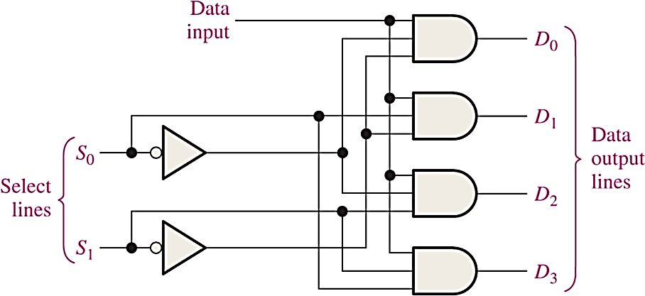
Demultiplexers (DEMUX) #
A DEMUX basically reverses the MUX function. It takes digital information from one line and distributes it to a given number of output lines. For this reason, the DEMUX is also known as a data distributer.
The figure below shows a 1-line-to-4-line DEMUX. The data-input line goes to “all” of the AND gates. The two data-selector lines enable only “one” gate at a time, and the data appearing on the data-input line will pass through the selected gate to the associated data-output line.
Summary #
- Half adder can be constructed with X-OR gate and AND gate
- ∑ = a b Cout = ab
- A full-adder can be constructed from two half adders and OR gate
- ∑ = (A B)+Cin Cout = AB + (A B) Cin
- Two or more full-adders are connected in parallel to form parallel binary adders
- A ripple carry adder is one in which the carry output of each full-adder is connected to the carry input of the next higher-order stage.
- To avoid carry propagation delay in ripple carry adder look-ahead carry adder anticipates the output carry of each stage
- In the simplest form, a comparator can test for equality using XNOR gates.
- The encoder and decoders are multi input multi output. An encoder accepts an active logic level on one of its inputs and converts it to a coded output, such as BCD or GRAY which is called encoding. Decoders performs exactly reverse function converts coded input to binary called decoding
- MUX has 2n data-input lines, n select line and a single output line. It connects one input line with output line depending on select line.
- DEMUX has 2n data-output lines, n select line and a single input line. It connects one output line with input line depending on select line.


